First off, where's the clock?
The Master Switch
Instead of operating on clock edges, an asynchronous design is implemented using a series of handshakes. In our CPU, almost every macroprocess is sequential, so the handshake is indicated simply by a digital high. Each process is preformed only when the start signal is high, and raises its finished signal when it is finished. Each subsequent process's start signal is wired directly to the finish of the previous process, allowing a chain reaction to propogate through.
When all the finish flags are up, it is time to move to the next instruction. To allow for this, a master switch is used, shown below.
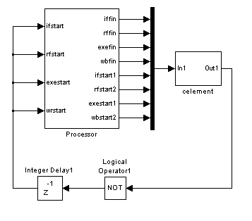
The start and finish signals are all put into a c-element, a latch-like element that raises high when all the inptus are high, low when all the inputs are low, and retains its previous state for any other input combination. If all the starts and finishes are high, then the c-element will rais a high. The starts will then be exerted low. A short time later, all the starts and finishes will also be low, and the c-element will output a high.
The start signal that's inputed into the processor is then and-gated to the finish signal of each previous process to produce the overall start input into the process, shown below
Since AND-gates give 0 when an input is 0, and is basically invisible when the input is 1, this allows us to control the shutting down of start signals, but not the turning on. Only when the chain reaction has completed will all the starts and finishes be exerted high again, and then the process will repeat.
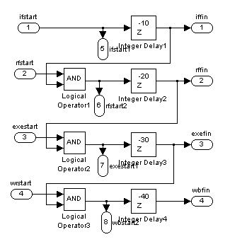
This idea was implemented on an overall CPU abstraction, shown before. Since each major step (instruction fetch (IF), register fetch (RF), execute (EXE), and write back (WB)) is composed of many little chain-reaction steps, we simply model the propagation delay of each process as a fixed delay.
CPU Overall Abstraction
The asynchronous CPU on a large scale is designed like a multicycle CPU. There are two major components: the dataflow and the control. In this project, we used behavioral code to implement the control, and used asynchronous hardware logic to implement the dataflow. The master switch is also shown here.

Figure 1: The overall processor
Dataflow
The overall CPU we designed is a very simplified version of the single-cycle CPU designed in Verilog for Computer Architecture. Only two instructions are used: add and xori. We chose to do this because this allowed for a significant reduction of CPU implementation complexity, and allowed us to focus on the asynchronous design instead. For example, with only these two instructions, the Data Memory is not used at all, and the PC will only ever increment up by 1 (or 4 LSBs). The major dataflow is shown below (click for larger view):

Figure 2: The dataflow in more detail
Each macro-process was then implemented using a series of MatLab embedded functions. Because the simulation software, Simulink, does not support composing a library of subsystems and allowing each copy of the subsystem to reference the same library copy, it was very difficult to make 32-bit ALUs and registers. By using a MatLab function, we could instead simulate the whole thing much more easily. We instead include smaller versions of a register, mux, and ALU, to show a proof of concept of their implementation. Included here are diagrams of each macroprocess (click for larger view). To see how each peice is implemented, go to the (DOWNLOAD PAGE LINK).
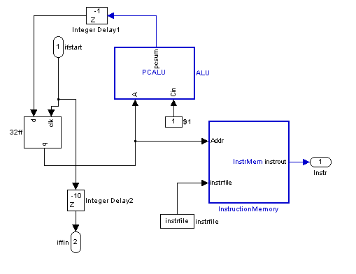
The instruction fetch (IF) unit |
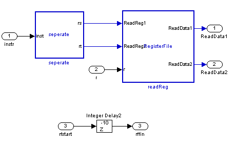
The register fetch (RF) and write back (WB) unit |
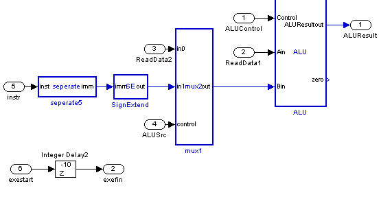
The execute (EXE) unit |
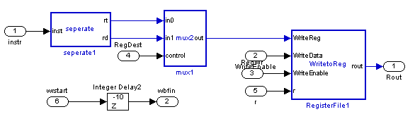
The write back (WB) unit |
Control
The controls include settings that decide things like what muxes should allow through, which operation an ALU should preform, etc. For our purposes, very few controls are needed. The logic is shown in the table below:
| Instruction | Op, funct |
ALUCtrl | ALUSrc | RegDest | RegWr |
| xori (immediate) | 14 | 10 | 1 | 0 | 1 |
| add (register) | 0,32 | 00 | 0 | 1 | 1 |
A simple assembly file that preforms adding was compiled and tested, and resulted in correct register content values.
The following image shows the simulation in use.
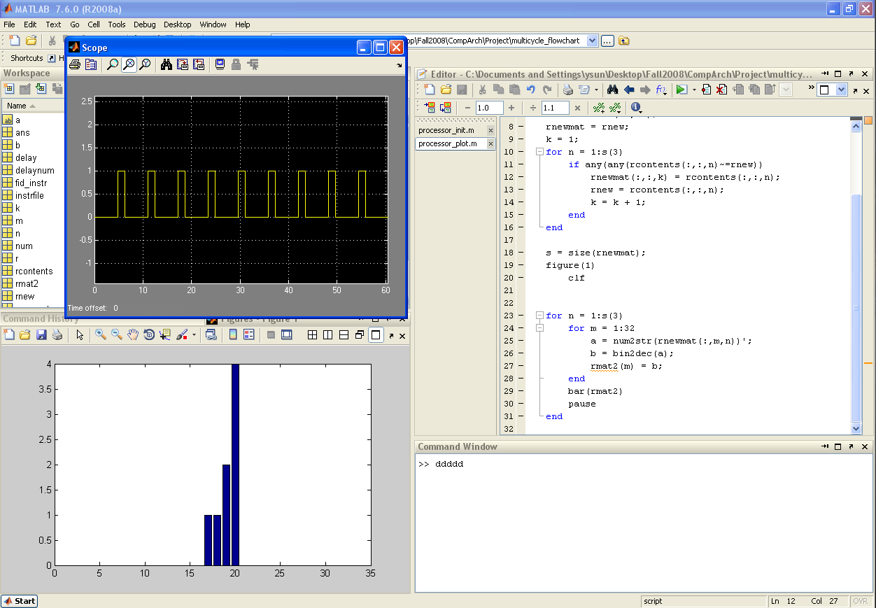
The bar plot shows the register contents ($s0 = 1, $s1 = 1, $s2 = 2, $s3 = 3, $s4 = 4), and the scope shows the master switch oscillation. (Click for larger image)